Board Overview
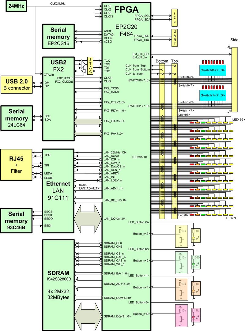
| This general schematic bloc diagram shows the different parts around the FPGA EP2C20 :
|
| USB2.0 interface with the Cypress FX2. This microcontroller communicate with the PC to download the content of the FPGA through the JTAG interface during the development phase of a design. It completely emulate the Byte-Blaster (Altera TM) interface. Thus it is possible to download FPGA content and memory content. It can be use too by the user to transfer data between USB and the FPGA for an user application. In this case a FIFO data transfert can be done between USB endpoint and the FPGA
|
| Ethernet interface through the LAN 91C111 and RJ45 connector.
|
| 32M Bytes of SDRAM (synchronous DRAM) organized in 4 banks of 2M words of 32 bits. A SDRAM controller has to be include in the FPGA to use it.
|
| 2 x 8 bits switches with associated LEDs. The FPGA can use the LED, the switch are not destructive in this case, thanks to a resistor network. The Switch/LED are connected to the side connectors. Switch0 to the Top connector too and Switch1 to the Bottom connector. The Switches/Leds are active High.
|
| 96 LEDs organized as a 12x8 matrix (or 8x12 as your application wish it). 48 LEDs are connected to the Top connector and 48 to the Bottom connector. The LEDs are active High.
|
| 4 independents switches buttons active low
|
| A single oscillator provide the Clock for the FPGA through 4 inputs, and to the FX2 microcontroller. The clock for the Ethernet as to be provide by the FPGA (25MHz) as for the SDRAM.
|
Board Schematic
Download the full schematics and layout of the board in PDF.
FPGA4U version B (old 08/2006)
FPGA4U version C (07/2007)
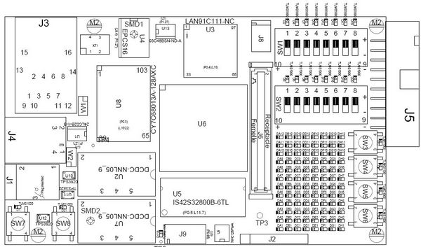
Board Components
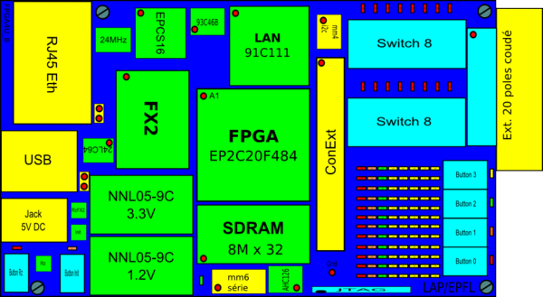
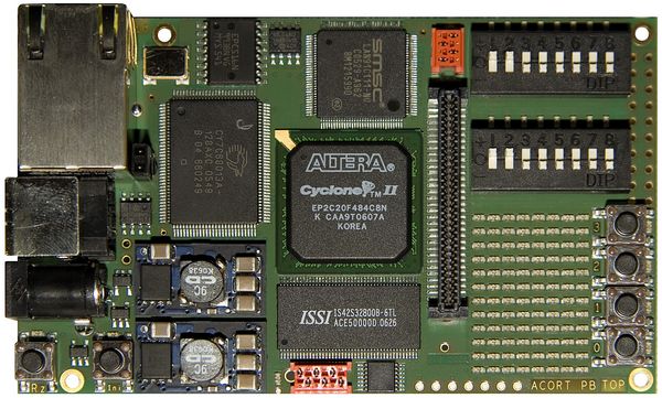
Top View
Components placement, Top View
|
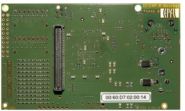
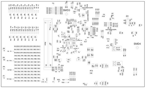
Bottom View
Components placement, Bottom View
|
Components
FPGA
The FPGA on the FPGA4U board is an Altera Cyclone II EP2C20. Package is F484 with 315 user IOs available. Speed grade is C8. If you are unsure you can check on your board. The FPGA chip should be labelled EP2C20F484C8.
Some revisions have speed grade C6 (they're faster) and are labeled EP2C20F484C6N.
Switches
The components SW1 and SW2 are made of 8 three state switches numbered on the device from 1: Switch_<7> at left to 8: Switch_0> at right. Each switch is associated with one LED which will turn on in case of a logic '1'. These LEDs can also be controlled by the FPGA by using the switch's pin as outputs. In this case the switches cannot be used a input signals.
- Switch0<7..0> are available on the TOP connector J6 and on the optional side connector J5.
|
- Switch1<7..0> are available on the BOTTOM connector J7 and on the optional side connector J5.
|
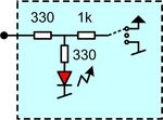 3 states switch and LED. The resistor network allow FPGA to win when opposite levels are provided.
Switches Pin Table
| SW1
|
| Pin Name |
Switch Nb |
FPGA Pin
|
| Switch0<7> |
1 |
PIN_E11
|
| Switch0<6> |
2 |
PIN_G11
|
| Switch0<5> |
3 |
PIN_F10
|
| Switch0<4> |
4 |
PIN_E9
|
| Switch0<3> |
5 |
PIN_H9
|
| Switch0<2> |
6 |
PIN_F8
|
| Switch0<1> |
7 |
PIN_H8
|
| Switch0<0> |
8 |
PIN_G7
|
|
| SW2
|
| Pin Name |
Switch Nb |
FPGA Pin
|
| Switch1<7> |
1 |
PIN_F11
|
| Switch1<6> |
2 |
PIN_H11
|
| Switch1<5> |
3 |
PIN_H10
|
| Switch1<4> |
4 |
PIN_F9
|
| Switch1<3> |
5 |
PIN_E8
|
| Switch1<2> |
6 |
PIN_G8
|
| Switch1<1> |
7 |
PIN_C7
|
| Switch1<0> |
8 |
PIN_H7
|
|
Push Buttons and LEDs (SW3 - SW6)
SW3 - SW6 are push buttons sending a logic « 0 » when pressed. Each button is normally associated with the LED next to it. These LEDs are not directly connected to the push-buttons and can only be controlled by the FPGA, a '1' light the LED.
SW3-6 & LED_SW3-6 Pin Table
| SW3-6
|
| Pin Name |
Button |
FPGA Pin
|
| Button_n<3> |
SW3 |
PIN_AB4
|
| Button_n<2> |
SW4 |
PIN_V12
|
| Button_n<1> |
SW5 |
PIN_U12
|
| Button_n<0> |
SW6 |
PIN_U11
|
|
| LED_SW3-6
|
| Pin Name |
LED |
FPGA Pin |
Color
|
| LED_Button<3> |
LED_SW3 |
PIN_AB20 |
Yellow
|
| LED_Button<2> |
LED_SW4 |
PIN_AA20 |
Green
|
| LED_Button<1> |
LED_SW5 |
PIN_AA17 |
Orange
|
| LED_Button<0> |
LED_SW6 |
PIN_Y16 |
Red
|
|
Clear and Reset Push-Buttons (SW7 - SW8)
| The 'Rz' push-button (SW7) can be used as reset for the system programmed in the FPGA. It doesn't reinitialize the FPGA configuration. The associated red LED light on when the switch is pushed. A reset generator chip (TPS3820-33) provide a clean active low 25 ms pulse.
|
| The 'Init' push-button (SW8) is used to reinitialise the FPGA and reload the configuration residing in the flash memory. An orange LED light on during the configuration time. When it light off, it means that the configuration is fully transfered in the FPGA. A reset generator chip (TPS3820-33) generate a clean pulse to the nCONFIG FPGA input when pressed. The associated orange LED is connected to the CONF_DONE FPGA signal. It means that the configuration is correctly loaded. The selected mode (MSEL1, MSEL0) is "00" for Asynchronous Serial.
|
SW7-8 & associated LED Pin Table
| Reset
|
| Switch Name |
Pin Name |
Button |
FPGA Pin
|
| Rz |
FPGA_Rz_n |
SW7 |
PIN_B3 (Dev_CLR_n)
|
| Init |
nCONFIG |
SW8 |
PIN_L4
|
|
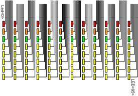
LED Array (LED[0] - LED[95])
The LED array contains the 96 elements organized in the following way:
LED Array Pin Table (Left Part)
| LED[0..7]
|
| LED N° |
FPGA Pin
|
| 0 |
PIN_Y18
|
| 1 |
PIN_Y20
|
| 2 |
PIN_Y22
|
| 3 |
PIN_W22
|
| 4 |
PIN_V20
|
| 5 |
PIN_V22
|
| 6 |
PIN_U20
|
| 7 |
PIN_U22
|
|
| LED[8..15]
|
| LED N° |
FPGA Pin
|
| 8 |
PIN_Y19
|
| 9 |
PIN_Y21
|
| 10 |
PIN_W21
|
| 11 |
PIN_V19
|
| 12 |
PIN_V21
|
| 13 |
PIN_U19
|
| 14 |
PIN_U21
|
| 15 |
PIN_T21
|
|
| LED[16..23]
|
| LED N° |
FPGA Pin
|
| 16 |
PIN_T22
|
| 17 |
PIN_R18
|
| 18 |
PIN_R20
|
| 19 |
PIN_R22
|
| 20 |
PIN_P17
|
| 21 |
PIN_N15
|
| 22 |
PIN_N22
|
| 23 |
PIN_M19
|
|
| LED[24..31]
|
| LED N° |
FPGA Pin
|
| 24 |
PIN_R17
|
| 25 |
PIN_R19
|
| 26 |
PIN_R21
|
| 27 |
PIN_P15
|
| 28 |
PIN_P18
|
| 29 |
PIN_N21
|
| 30 |
PIN_M18
|
| 31 |
PIN_L18
|
|
| LED[32..39]
|
| LED N° |
FPGA Pin
|
| 32 |
PIN_T6
|
| 33 |
PIN_R7
|
| 34 |
PIN_P3
|
| 35 |
PIN_J2
|
| 36 |
PIN_H6
|
| 37 |
PIN_H4
|
| 38 |
PIN_H2
|
| 39 |
PIN_G6
|
|
| LED[40..47]
|
| LED N° |
FPGA Pin
|
| 40 |
PIN_U3
|
| 41 |
PIN_R8
|
| 42 |
PIN_R6
|
| 43 |
PIN_J4
|
| 44 |
PIN_J1
|
| 45 |
PIN_H5
|
| 46 |
PIN_H3
|
| 47 |
PIN_H1
|
|
LED Array Pin Table (Right part)
| LED[48..55]
|
| LED N° |
FPGA Pin
|
| 48 |
PIN_G3
|
| 49 |
PIN_F3
|
| 50 |
PIN_F1
|
| 51 |
PIN_E3
|
| 52 |
PIN_E1
|
| 53 |
PIN_D3
|
| 54 |
PIN_D1
|
| 55 |
PIN_C1
|
|
| LED[56..63]
|
| LED N° |
FPGA Pin
|
| 56 |
PIN_G5
|
| 57 |
PIN_F4
|
| 58 |
PIN_F2
|
| 59 |
PIN_E4
|
| 60 |
PIN_E2
|
| 61 |
PIN_D4
|
| 62 |
PIN_D2
|
| 63 |
PIN_C2
|
|
| LED[64..71]
|
| LED N° |
FPGA Pin
|
| 64 |
PIN_K20
|
| 65 |
PIN_K22
|
| 66 |
PIN_J17
|
| 67 |
PIN_J19
|
| 68 |
PIN_J21
|
| 69 |
PIN_H16
|
| 70 |
PIN_H18
|
| 71 |
PIN_G17
|
|
| LED[72..79]
|
| LED N° |
FPGA Pin
|
| 72 |
PIN_K21
|
| 73 |
PIN_J15
|
| 74 |
PIN_J18
|
| 75 |
PIN_J20
|
| 76 |
PIN_J22
|
| 77 |
PIN_H17
|
| 78 |
PIN_H19
|
| 79 |
PIN_G18
|
|
| LED[80..87]
|
| LED N° |
FPGA Pin
|
| 80 |
PIN_G21
|
| 81 |
PIN_F20
|
| 82 |
PIN_F22
|
| 83 |
PIN_E21
|
| 84 |
PIN_D19
|
| 85 |
PIN_D21
|
| 86 |
PIN_C19
|
| 87 |
PIN_C21
|
|
| LED[88..95]
|
| LED N° |
FPGA Pin
|
| 88 |
PIN_G22
|
| 89 |
PIN_F21
|
| 90 |
PIN_E20
|
| 91 |
PIN_E22
|
| 92 |
PIN_D20
|
| 93 |
PIN_D22
|
| 94 |
PIN_C20
|
| 95 |
PIN_C22
|
|
| The 12 LED[0+n*8] are Red.
|
| The 12 LED[1+n*8] are Orange.
|
| The 12 LED[2+n*8] are Green.
|
| The 5*12 LED[3,4,5,6,7 + n*8] are Yellow.
|
Depending on the pin assignment made, they can be seen as 8*12 matrix or 12*8 matrix.
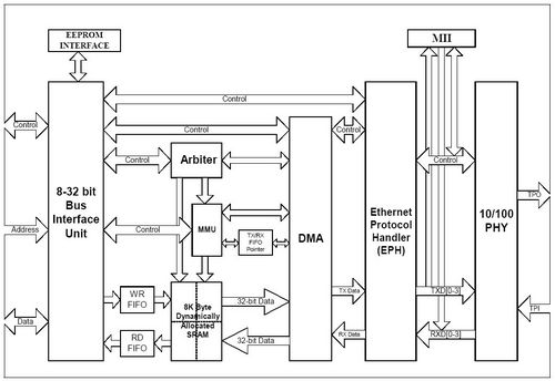
LAN91C111 (U3)
The LAN91C111 is a MAC+PHY interface for 10/100 Mbits Ethernet RJ-45 interface. It has the responsibility of packet transfers under a processor control. The processor has to be included in the FPGA with the software.
A serial memory is programmed with the EPFL MAC address. The 16 bits lowest address is the FPGA4U serial number.
The LAN is decoded at address 0x300 with AD<15..A5>, by external Pull_up and Pull_down. This base address must NOT be change in the internal Bank1, offset 2, BASE register of the 91C111. The AD<15..5> are not connected to the FPGA.
The LAN_25MHz_Clk need to be generated by a PLL receiving its input Clk from Clk8_24MHz, pin B12.
LAN91C111 Pin Table
| Name |
FPGA Pin |
Remark
|
| LAN_25MHz_Clk |
PIN_D5 |
from FPGA, 25MHz Clock
|
| LAN_Reset |
PIN_E7 |
from FPGA, Reset active high
|
| LAN_IOR_n |
PIN_B4 |
from FPGA, Read cycle from FPGA
|
| LAN_IOW_n |
PIN_A4 |
from FPGA, Write cycle from FPGA
|
| LAN_DATACS_n |
PIN_A6 |
from FPGA, Data access 32 bits at a time (BE_n[3..0] not used)
|
| LAN_AEN_n |
PIN_A11 |
from FPGA, Address Enable, to be left open (pull-down) or put at '0'
|
| LAN_ARDY |
PIN_A9 |
to FPGA, Asynchronous ready (Ready when '1'), open drain
|
| LAN_INT |
PIN_A3 |
to FPGA, Interrupt Request ('1')
|
| LAN_LDEV_n |
PIN_A13 |
to FPGA, LAN correctly decoded
|
| LAN_AD[1] |
PIN_B11 |
from FPGA, Address low, 16 bits word
|
| LAN_AD[2] |
PIN_D11 |
|
| LAN_AD[3] |
PIN_A10 |
|
| LAN_AD[4] |
PIN_B10 |
|
| LAN_BE_n[0] |
PIN_B9 |
from FPGA, Byte Enable D[7..0]
|
| LAN_BE_n[1] |
PIN_C9 |
from FPGA, Byte Enable D[15..8]
|
| LAN_BE_n[2] |
PIN_A8 |
from FPGA, Byte Enable D[23..16]
|
| LAN_BE_n[3] |
PIN_B8 |
from FPGA, Byte Enable D[31..24]
|
|
| Name |
FPGA Pin |
Remark
|
| LAN_DQ[0] |
PIN_B5 |
Data bidirectional
|
| LAN_DQ[1] |
PIN_A5 |
|
| LAN_DQ[2] |
PIN_D7 |
|
| LAN_DQ[3] |
PIN_B6 |
|
| LAN_DQ[4] |
PIN_D8 |
|
| LAN_DQ[5] |
PIN_B7 |
|
| LAN_DQ[6] |
PIN_A7 |
|
| LAN_DQ[7] |
PIN_D9 |
|
| LAN_DQ[8] |
PIN_E14 |
|
| LAN_DQ[9] |
PIN_B13 |
|
| LAN_DQ[10] |
PIN_D14 |
|
| LAN_DQ[11] |
PIN_C14 |
|
| LAN_DQ[12] |
PIN_A14 |
|
| LAN_DQ[13] |
PIN_B14 |
|
| LAN_DQ[14] |
PIN_F14 |
|
| LAN_DQ[15] |
PIN_E15 |
|
|
| Name |
FPGA Pin |
Remark
|
| LAN_DQ[16] |
PIN_A20 |
not for registers access
|
| LAN_DQ[17] |
PIN_B20 |
DQ[31..16]
|
| LAN_DQ[18] |
PIN_B19 |
|
| LAN_DQ[19] |
PIN_A19 |
|
| LAN_DQ[20] |
PIN_C18 |
|
| LAN_DQ[21] |
PIN_B18 |
|
| LAN_DQ[22] |
PIN_A18 |
|
| LAN_DQ[23] |
PIN_C17 |
|
| LAN_DQ[24] |
PIN_B17 |
|
| LAN_DQ[25] |
PIN_A17 |
|
| LAN_DQ[26] |
PIN_D16 |
|
| LAN_DQ[27] |
PIN_B16 |
|
| LAN_DQ[28] |
PIN_A16 |
|
| LAN_DQ[29] |
PIN_D15 |
|
| LAN_DQ[30] |
PIN_B15 |
|
| LAN_DQ[31] |
PIN_A15 |
|
|
Internal architecture of LAN91C111 interface. A specific memory array provide buffer for receive and transmit data. The access to this memory can be done 32 bits at a time.
LAN91C111 Block Diagram
|
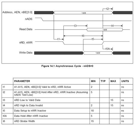
Transfers diagrams from smsc LAN91C111 documentation.
LAN91C111 Read Write access
|
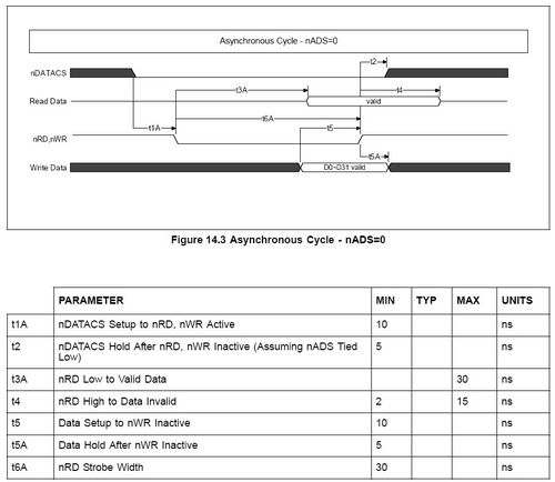
The configuration of the circuit is done through 16 bits access registers transfers. A special 32 bits access can be done to transfers data from internal buffer memory with the DATA_CS_n signal.
LAN91C111 Read Write DataCS access
|
Component on SOPC Builder
Using SOPC Builder with the NIOSII processor, the Avalon-MM Tristate Bridge needs to be connected to the LAN91C111 component MAC/PHY on development board.
EPCS16 (U4)
This EPCS16 serial memory from Altera can have a full design for configuration of the CycloneII FPGA. The content is transfered during the Configuration phase at power up or when the Init button is pressed. To be able to program it, a design must incorporate an epcs_controller. If you simply want to modify the design configuration that is loaded at power up, take a look at the page EPCS_Loader.
|
Special signal lines are reserved on the FPGA to connect this component.
|
SDRAM (U5)
The SDRAM is an ISSI IS42S32800B. With 32 bits data bus, validated by SDRAM_DQM<3..0> signals, one for each Byte of data bus SDRAM_DQ<31..0>.
This memory is a synchronous SDRAM, validating address and control signals with the rising edge of SDRAM_CLK, while SDRAM_CKE activated ('1').
The organisation is 4 banks selected by SDRAM_BA<1..0>. Each bank as 2^12 Row and 2^9 Column selected by SDRAM_AD<11.0>, with 32 bits words (SDRAM_DQ<31..0> (2^2 * 2^12 * 2^9 = 4 * 2M x 32 = 8Mx32 = 32MBytes).
|
In SOPC Builder, with the SDRAM Controller, select:
|
- 12 Rows addresses lines
|
- 9 Columns addresses lines
|
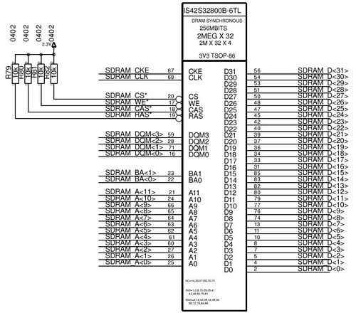
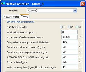
SDRAM Pin Table
| Name |
FPGA Pin
|
| SDRAM_BA[0] |
PIN_Y10
|
| SDRAM_BA[1] |
PIN_AB11
|
| |
.
|
| SDRAM_AD[0] |
PIN_AB13
|
| SDRAM_AD[1] |
PIN_U13
|
| SDRAM_AD[2] |
PIN_U14
|
| SDRAM_AD[3] |
PIN_V15
|
| SDRAM_AD[4] |
PIN_V14
|
| SDRAM_AD[5] |
PIN_Y13
|
| SDRAM_AD[6] |
PIN_AA12
|
| SDRAM_AD[7] |
PIN_AA11
|
| SDRAM_AD[8] |
PIN_W11
|
| SDRAM_AD[9] |
PIN_U9
|
| SDRAM_AD[10] |
PIN_AB12
|
| SDRAM_AD[11] |
PIN_U8
|
|
| Name |
FPGA Pin
|
| SDRAM_DQ[0] |
PIN_W7
|
| SDRAM_DQ[1] |
PIN_AB6
|
| SDRAM_DQ[2] |
PIN_AA7
|
| SDRAM_DQ[3] |
PIN_W8
|
| SDRAM_DQ[4] |
PIN_V9
|
| SDRAM_DQ[5] |
PIN_AA9
|
| SDRAM_DQ[6] |
PIN_U10
|
| SDRAM_DQ[7] |
PIN_AB10
|
| SDRAM_DQ[8] |
PIN_V11
|
| SDRAM_DQ[9] |
PIN_AA10
|
| SDRAM_DQ[10] |
PIN_AB9
|
| SDRAM_DQ[11] |
PIN_AB8
|
| SDRAM_DQ[12] |
PIN_AA8
|
| SDRAM_DQ[13] |
PIN_AB7
|
| SDRAM_DQ[14] |
PIN_V8
|
| SDRAM_DQ[15] |
PIN_AA6
|
|
| Name |
FPGA Pin
|
| SDRAM_DQ[16] |
PIN_W14
|
| SDRAM_DQ[17] |
PIN_AB14
|
| SDRAM_DQ[18] |
PIN_AB15
|
| SDRAM_DQ[19] |
PIN_AA15
|
| SDRAM_DQ[20] |
PIN_AB16
|
| SDRAM_DQ[21] |
PIN_W16
|
| SDRAM_DQ[22] |
PIN_Y17
|
| SDRAM_DQ[23] |
PIN_AB19
|
| SDRAM_DQ[24] |
PIN_AA19
|
| SDRAM_DQ[25] |
PIN_AA18
|
| SDRAM_DQ[26] |
PIN_AB18
|
| SDRAM_DQ[27] |
PIN_AA16
|
| SDRAM_DQ[28] |
PIN_W15
|
| SDRAM_DQ[29] |
PIN_Y14
|
| SDRAM_DQ[30] |
PIN_AA14
|
| SDRAM_DQ[31] |
PIN_AA13
|
|
| Name |
FPGA Pin
|
| SDRAM_Clk |
PIN_U4
|
| SDRAM_CKE |
PIN_W9
|
| |
.
|
| SDRAM_CS_n |
PIN_Y7
|
| SDRAM_RAS_n |
PIN_Y6
|
| SDRAM_CAS_n |
PIN_Y5
|
| SDRAM_WE_n |
PIN_AA5
|
| |
.
|
| SDRAM_DQM[0] |
PIN_AB5
|
| SDRAM_DQM[1] |
PIN_Y9
|
| SDRAM_DQM[2] |
PIN_AB17
|
| SDRAM_DQM[3] |
PIN_U15
|
|
SDRAM Clk
To use the SDRAM, a clk is necessary. It must be provided with the same frequency and phase as the CPU (NIOS II in general) and Avalon bus if used with SOPC Builder.
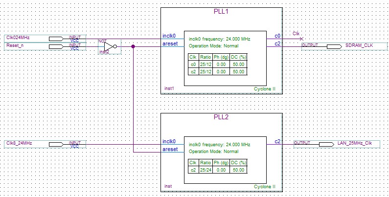
In general the Clk is provided by a PLL module from the 24MHz clock at 50 MHz.
The ALTPLL from the MegaWizard Plug-In Manager is to be include. With Feedback path inside the PLL in normal mode.
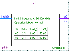
From the figure :
- inclk0 <-- Clk0_24MHz
- c0 --> clk of the NIOS module
- c2 --> SDRAM_Clk !! not c1 !!
FX2 (U8)
| The FX2 FX2 LP 68013Ais a microcontroller based on the 8051 microprocessor and a specific USB2.0 Full Speed (12 Mbps) and High Speed (480 Mbps) engines. It is used to program the FPGA by JTAG transfers and to communicate with the FPGA through high speed FIFO or GPIF interface (General Purpose Interface Protocol) from Cypress.
By default the FIFO mode is programmed in the Firmware in the FX2 on FPGA4U board.
|
| The GPIF transfers are controlled by a state machine in the FX2 chip.
|
| The FX2_CTL[2..0] and FX2_RDY[1..0] pins are available for this function.
|
| The data transfers can be 16 bits at a time.
|
FX2 Pin Table
| Name |
FPGA Pin |
Remark
|
| FX2_CLKOut |
PIN_M1 |
CLK2 FPGA input
|
| FX2_IFCLK |
PIN_M2 |
CLK3 FPGA input
|
| FX2_CTL[0] |
PIN_N6 |
FX2 GPIF output
|
| FX2_CTL[1] |
PIN_N4 |
FX2 GPIF output
|
| FX2_CTL[2] |
PIN_P6 |
FX2 GPIF output
|
| FX2_Rdy[0] |
PIN_M6 |
FX2 GPIF input
|
| FX2_Rdy[1] |
PIN_M5 |
FX2 GPIF input
|
| FX2_RxD0 |
PIN_Y3 |
FX2 RxD serial UART
|
| FX2_TxD0 |
PIN_Y2 |
FX2 TxD serial UART
|
| FX2_PA[0] |
PIN_W5 |
FX2 INT0_n, or PIO
|
| FX2_PA[1] |
PIN_U1 |
FX2 INT1_n, or PIO
|
| FX2_PA[2] |
PIN_U2 |
FX2 SLOE, or PIO
|
| FX2_PA[3] |
PIN_T1 |
FX2 WU2, or PIO
|
| FX2_PA[4] |
PIN_T2 |
FX2 FIFOAdr0, or PIO
|
| FX2_PA[5] |
PIN_T3 |
FX2 FIFOAdr1, or PIO
|
| FX2_PA[6] |
PIN_T5 |
FX2 PKTEND, or PIO
|
| FX2_PA[7] |
PIN_R1 |
FX2 SLCS_n, or PIO
|
|
| Name |
FPGA Pin |
Remark
|
| FX2_FD[0] |
PIN_Y1 |
FIFO Data, or GPIF Data
|
| FX2_FD[1] |
PIN_Y4 |
FIFO Data, or GPIF Data
|
| FX2_FD[2] |
PIN_W4 |
FIFO Data, or GPIF Data
|
| FX2_FD[3] |
PIN_W1 |
FIFO Data, or GPIF Data
|
| FX2_FD[4] |
PIN_W2 |
FIFO Data, or GPIF Data
|
| FX2_FD[5] |
PIN_W3 |
FIFO Data, or GPIF Data
|
| FX2_FD[6] |
PIN_V1 |
FIFO Data, or GPIF Data
|
| FX2_FD[7] |
PIN_V2 |
FIFO Data, or GPIF Data
|
| FX2_FD[8] |
PIN_N3 |
FIFO Data, or GPIF Data
|
| FX2_FD[9] |
PIN_N2 |
FIFO Data, or GPIF Data
|
| FX2_FD[10] |
PIN_N1 |
FIFO Data, or GPIF Data
|
| FX2_FD[11] |
PIN_P5 |
FIFO Data, or GPIF Data
|
| FX2_FD[12] |
PIN_P2 |
FIFO Data, or GPIF Data
|
| FX2_FD[13] |
PIN_P1 |
FIFO Data, or GPIF Data
|
| FX2_FD[14] |
PIN_R5 |
FIFO Data, or GPIF Data
|
| FX2_FD[15] |
PIN_R2 |
FIFO Data, or GPIF Data
|
|
| The FIFO transfers are under the control of the FPGA after initialization by the FX2. Control signals from PA[7..0] are used. With FIFO mode, FIFOAdr0[1..0] specify the Endpoint to be used.
|
| Access are controlled by SLRD_n, SLWR_n signals for read/write transfers. In FIFO mode, the FPGA is the master of the transfers. SLOE_n is used to enabled the tri-state FD bus in output from the FX2.
|
FX2 FIFO Ctrl Pin Table
| Name |
FPGA Pin |
Remark
|
| FX2_CTL[0] |
PIN_N6 |
FX2_FIFO_FlagA, programmable signal
|
| FX2_CTL[1] |
PIN_N4 |
FX2_FIFO_FlagB, or FIFO_FULL_n
|
| FX2_CTL[2] |
PIN_P6 |
FX2_FIFO_FlagC, or FIFO_EMPTY_n
|
| FX2_Rdy[0] |
PIN_M6 |
FX2_FIFO_SLRD_n
|
| FX2_Rdy[1] |
PIN_M5 |
FX2_FIFO_SLWR_n
|
| FX2_PA[2] |
PIN_U2 |
FX2_FIFO_SLOE_n
|
| FX2_PA[4] |
PIN_T2 |
FX2_FIFO_FIFOAdr0
|
| FX2_PA[5] |
PIN_T3 |
FX2_FIFO_FIFOAdr1
|
| FX2_PA[6] |
PIN_T5 |
FX2_FIFO_PktEnd
|
|
Port JTAG (J2)
This connector is optional. It is provide for specific application with a direct access to the FPGA JTAG connexion and FX2 access disabled (PC7 = FX2_JTAG_E = '0' as output, or configured as input).
|
An adapter can easily be done for a Byte-Blaster JTAG interface, as we can see the corresponding 7 pins 0.1" and 2 rows 10 pins 0.1" connector. It is possible to use a 2 rows 14 pins connector
|
JTAG 7 pins vs Byte-Blaster 10 Pins Table
|
|
| JTAG Pin Table
|
| Pin Num |
Name |
FPGA Pin
|
| 1 |
TCK |
PIN_K2
|
| 2 |
TDO |
PIN_L5
|
| 3 |
TMS |
PIN_K6
|
| 4 |
. |
|
| 5 |
TDI |
PIN_K5
|
| 6 |
3.3V |
|
| 7 |
Gnd |
|
|
| Byte-Blaster JTAG...
|
| Pin Num |
Name
|
| 1 |
TCK
|
| 3 |
TDO
|
| 5 |
TMS
|
| 7 |
.
|
| 9 |
TDI
|
|
| ... 10 Pins Table
|
| Pin Num |
Name
|
| 2 |
Gnd
|
| 4 |
3.3V
|
| 6 |
.
|
| 8 |
.
|
| 10 |
Gnd
|
|
| Byte-Blaster JTAG adapter...
|
| Pin Num |
Name
|
| 1 |
TCK
|
| 3 |
TDO
|
| 5 |
TMS
|
| 7 |
.
|
| 9 |
TDI
|
| 11 |
3.3V
|
| 13 |
Gnd
|
|
| ... 14 Pins Table
|
| Pin Num |
Name
|
| 2 |
Gnd
|
| 4 |
3.3V
|
| 6 |
.
|
| 8 |
.
|
| 10 |
Gnd
|
| 12 |
.
|
| 14 |
.
|
|
Port 20 Pins (2x10)(J5)
| The 20 pins port is optional. It allows the connection of external devices such as cameras, various acquisition modules and Mubus interfaces to the FPGA4U board.
|
Port 2x10 Pin Table
| Pin Num |
Name |
FPGA Pin |
FPGA function
|
| 1 |
3.3V |
|
|
| 3 |
Ext_Clk_In |
PIN_U18 |
IO/PLL4_OUTn
|
| 5 |
SWITCH0[1] |
PIN_H8 |
|
| 7 |
SWITCH0[3] |
PIN_H9 |
|
| 9 |
SWITCH0[5] |
PIN_F10 |
|
| 11 |
SWITCH0[7] |
PIN_E11 |
|
| 13 |
SWITCH1[1] |
PIN_C7 |
|
| 15 |
SWITCH1[3] |
PIN_E8 |
|
| 17 |
SWITCH1[5] |
PIN_H10 |
|
| 19 |
SWITCH1[7] |
PIN_F11 |
|
|
| Pin Num |
Name |
FPGA Pin |
FPGA function
|
| 2 |
Ext_Clk_Out |
PIN_T18 |
IO/PLL4_OUTp
|
| 4 |
SWITCH0[0] |
PIN_G7 |
|
| 6 |
SWITCH0[2] |
PIN_F8 |
|
| 8 |
SWITCH0[4] |
PIN_E9 |
|
| 10 |
SWITCH0[6] |
PIN_G11 |
|
| 12 |
SWITCH1[0] |
PIN_H7 |
|
| 14 |
SWITCH1[2] |
PIN_G8 |
|
| 16 |
SWITCH1[4] |
PIN_F9 |
|
| 18 |
SWITCH1[6] |
PIN_H11 |
|
| 20 |
Gnd |
|
|
|
note: pin 1 (+3.3V) is in the top right corner (hole with a square frame).
Top 64 pins receptacle female connector (J6)
The connectors are 64 pins from Molex.
It's call receptacle or female.
The model is 71439-3*** with a height of 10.30 mm. Associated with the plug connector 71436_2*** of 8.35 mm, the board to board distance is 15.0 mm.
The maximum voltage that can be applied as Input is 4.0V on all I/O pins.
Port 64 Pin receptacle Table TOP view pins numbering with FPGA at the left of the connector, look on component placement [1]
| Pin Num |
Name |
FPGA Pin |
Alternate function
|
| 1 |
|
3.3V |
|
| 3 |
PIN_E19 |
CLK_to_Conn |
|
| 5 |
PIN_G7 |
SWITCH0[0] |
|
| 7 |
PIN_F8 |
SWITCH0[2] |
|
| 9 |
PIN_E9 |
SWITCH0[4] |
|
| 11 |
PIN_G11 |
SWITCH0[6] |
|
| 13 |
|
Gnd |
|
| 15 |
PIN_C21 |
LED[87] |
|
| 17 |
PIN_D21 |
LED[85] |
|
| 19 |
PIN_E21 |
LED[83] |
|
| 21 |
PIN_F20 |
LED[81] |
|
| 23 |
PIN_G17 |
LED[71] |
|
| 25 |
PIN_H16 |
LED[69] |
|
| 27 |
PIN_J19 |
LED[67] |
|
| 29 |
PIN_K22 |
LED[65] |
|
| 31 |
PIN_C1 |
LED[55] |
|
| 33 |
PIN_D3 |
LED[53] |
|
| 35 |
PIN_E3 |
LED[51] |
|
| 37 |
PIN_F3 |
LED[49] |
|
| 39 |
PIN_G6 |
LED[39] |
|
| 41 |
PIN_H4 |
LED[37] |
|
| 43 |
PIN_J2 |
LED[35] |
|
| 45 |
PIN_R7 |
LED[33] |
|
| 47 |
PIN_M19 |
LED[23] |
|
| 49 |
PIN_N15 |
LED[21] |
|
| 51 |
PIN_R22 |
LED[19] |
|
| 53 |
PIN_R18 |
LED[17] |
|
| 55 |
PIN_U22 |
LED[7] |
CDPCLK4/ DQS3R
|
| 57 |
PIN_V22 |
LED[5] |
|
| 59 |
PIN_W22 |
LED[3] |
|
| 61 |
PIN_Y20 |
LED[1] |
|
| 63 |
|
Gnd |
|
|
| Pin Num |
Name |
FPGA Pin |
Alternate function
|
| 2 |
|
3.3V |
|
| 4 |
PIN_L22 |
CLK_from_top |
|
| 6 |
PIN_H8 |
SWITCH0[1] |
|
| 8 |
PIN_H9 |
SWITCH0[3] |
|
| 10 |
PIN_F10 |
SWITCH0[5] |
|
| 12 |
PIN_E11 |
SWITCH0[7] |
|
| 14 |
|
Gnd |
|
| 16 |
PIN_C19 |
LED[86] |
|
| 18 |
PIN_D19 |
LED[84] |
|
| 20 |
PIN_F22 |
LED[82] |
CDPCLK5/ DQS2R
|
| 22 |
PIN_G21 |
LED[80] |
|
| 24 |
PIN_H18 |
LED[70] |
|
| 26 |
PIN_J21 |
LED[68] |
|
| 28 |
PIN_J17 |
LED[66] |
|
| 30 |
PIN_K20 |
LED[64] |
|
| 32 |
PIN_D1 |
LED[54] |
|
| 34 |
PIN_E1 |
LED[52] |
|
| 36 |
PIN_F1 |
LED[50] |
|
| 38 |
PIN_G3 |
LED[48] |
|
| 40 |
PIN_H2 |
LED[38] |
|
| 42 |
PIN_H6 |
LED[36] |
|
| 44 |
PIN_P3 |
LED[34] |
|
| 46 |
PIN_T6 |
LED[32] |
|
| 48 |
PIN_N22 |
LED[22] |
|
| 50 |
PIN_P17 |
LED[20] |
|
| 52 |
PIN_R20 |
LED[18] |
|
| 54 |
PIN_T22 |
LED[16] |
|
| 56 |
PIN_U20 |
LED[6] |
|
| 58 |
PIN_V20 |
LED[4] |
|
| 60 |
PIN_Y22 |
LED[2] |
|
| 62 |
PIN_Y18 |
LED[0] |
|
| 64 |
|
Gnd |
|
|
Bottom 64 pins plug male connector (J7)
The connectors are 64 pins from Molex. With the connecting physical standard ieee 1386. It's call plug or male.
The model is the plug connector 71436_2*** of 8.35 mm. Associated with the receptacle 71439-3*** with a height of 10.30 mm, the board to board distance is 15.0 mm.
The maximum voltage that can be applied as Input is 4.0V on all I/O pins.
Look on component placement [2] for orientation.
The pins x bottom's connector is in front of the Top connector pins x but not directly connected.
|
Port 64 Pin plug Table Bottom view pins numbering with FPGA holes at the right of the connector
| Pin Num
|
Name
|
FPGA Pin
|
Alternate function
|
FPGARM4U function
|
| 2
|
|
3.3V
|
|
3.3V
|
| 4
|
PIN_E19
|
CLK_to_Conn
|
|
CLK from FPGA4U
|
| 6
|
PIN_C7
|
SWITCH1[1]
|
|
PE17
|
| 8
|
PIN_E8
|
SWITCH1[3]
|
|
PE16
|
| 10
|
PIN_H10
|
SWITCH1[5]
|
|
nReset
|
| 12
|
PIN_F11
|
SWITCH1[7]
|
|
SPI1 nPCS1
|
| 14
|
|
Gnd
|
|
GND
|
| 16
|
PIN_C20
|
LED[94]
|
|
EBI1_D15
|
| 18
|
PIN_D20
|
LED[92]
|
|
EBI1_D13
|
| 20
|
PIN_E20
|
LED[90]
|
|
EBI1_D11
|
| 22
|
PIN_G22
|
LED[88]
|
|
EBI1_D9
|
| 24
|
PIN_H19
|
LED[78]
|
|
EBI1_D7
|
| 26
|
PIN_J22
|
LED[76]
|
|
EBI1_D5
|
| 28
|
PIN_J18
|
LED[74]
|
|
EBI1_D3
|
| 30
|
PIN_K21
|
LED[72]
|
|
EBI1_D1
|
| 32
|
PIN_D2
|
LED[62]
|
|
EBI1_nRD
|
| 34
|
PIN_E2
|
LED[60]
|
|
EBI1_nWR1
|
| 36
|
PIN_F2
|
LED[58]
|
|
EBI1_A22
|
| 38
|
PIN_G5
|
LED[56]
|
|
EBI1_A20
|
| 40
|
PIN_H3
|
LED[46]
|
|
EBI1_A17
|
| 42
|
PIN_J1
|
LED[44]
|
DPCLK0/ DQS0L
|
PCK0
|
| 44
|
PIN_R6
|
LED[42]
|
|
EBI1_A15
|
| 46
|
PIN_U3
|
LED[40]
|
|
EBI1_A13
|
| 48
|
PIN_M18
|
LED[30]
|
DPCLK6/ DQS1R
|
EBI1_A11
|
| 50
|
PIN_P18
|
LED[28]
|
|
EBI1_A9
|
| 52
|
PIN_R21
|
LED[26]
|
|
EBI1_A7
|
| 54
|
PIN_R17
|
LED[24]
|
|
EBI1_A5
|
| 56
|
PIN_U21
|
LED[14]
|
|
EBI1_A3
|
| 58
|
PIN_V21
|
LED[12]
|
|
EBI1_A1
|
| 60
|
PIN_W21
|
LED[10]
|
|
EBI1_nWait
|
| 62
|
PIN_Y19
|
LED[8]
|
|
IRQ
|
| 64
|
|
Gnd
|
|
GND
|
|
| Pin Num |
Name |
FPGA Pin |
Alternate function |
FPGARM4U function
|
| 1
|
|
3.3V
|
|
3.3V
|
| 3
|
PIN_M22
|
CLK_from_bottom
|
|
PCK0
|
| 5
|
PIN_H7
|
SWITCH1[0]
|
|
SPI1_MOSI
|
| 7
|
PIN_G8
|
SWITCH1[2]
|
|
SPI1_SPCK
|
| 9
|
PIN_F9
|
SWITCH1[4]
|
|
SPI1_MISO
|
| 11
|
PIN_H11
|
SWITCH1[6]
|
|
SPI1_nPCS0
|
| 13
|
|
Gnd
|
|
GND
|
| 15
|
PIN_C22
|
LED[95]
|
|
EBI1_nCS2
|
| 17
|
PIN_D22
|
LED[93]
|
|
EBI1_D14
|
| 19
|
PIN_E22
|
LED[91]
|
|
EBI1_D12
|
| 21
|
PIN_F21
|
LED[89]
|
|
EBI1_D10
|
| 23
|
PIN_G18
|
LED[79]
|
|
EBI1_D8
|
| 25
|
PIN_H17
|
LED[77]
|
|
EBI1_D6
|
| 27
|
PIN_J20
|
LED[75]
|
|
EBI1_D4
|
| 29
|
PIN_J15
|
LED[73]
|
|
EBI1_D2
|
| 31
|
PIN_C2
|
LED[63]
|
|
EBI1_D0
|
| 33
|
PIN_D4
|
LED[61]
|
|
EBI1_nWR0
|
| 35
|
PIN_E4
|
LED[59]
|
|
EBI1_nCS0
|
| 37
|
PIN_F4
|
LED[57]
|
|
EBI1_A21
|
| 39
|
PIN_H1
|
LED[47]
|
|
EBI1_A19
|
| 41
|
PIN_H5
|
LED[45]
|
CDPCLK0/ DQS2L
|
EBI1_A18
|
| 43
|
PIN_J4
|
LED[43]
|
|
EBI1_A16
|
| 45
|
PIN_R8
|
LED[41]
|
|
EBI1_A14
|
| 47
|
PIN_L18
|
LED[31]
|
DPCLK7/ DQS0R
|
EBI1_A12
|
| 49
|
PIN_N21
|
LED[29]
|
|
EBI1_A10
|
| 51
|
PIN_P15
|
LED[27]
|
|
EBI1_A8
|
| 53
|
PIN_R19
|
LED[25]
|
|
EBI1_A6
|
| 55
|
PIN_T21
|
LED[15]
|
|
EBI1_A4
|
| 57
|
PIN_U19
|
LED[13]
|
|
EBI1_A2
|
| 59
|
PIN_V19
|
LED[11]
|
|
EBI1_A0
|
| 61
|
PIN_Y21
|
LED[9]
|
|
DMA
|
| 63
|
|
Gnd
|
|
GND
|
|
I2C Port (J8)
| The i2c interface is simply a 4 pins connector to be used with camera interface.
|
I2C Port Pin Table
| Pin Num |
Name |
FPGA Pin
|
| 1 |
Gnd |
|
| 2 |
3.3V |
|
| 3 |
SDA |
PIN_C13
|
| 4 |
SCL |
PIN_C16
|
Serial Port (J9)
The UART serial connector is a 6 pins micro match connector for flat cable extension. The RokSer serial module interface is an adapter for RS-232 available for this extension. It allow a connection to a PC for serial transfers. An UART interface has to be implemented in the FPGA for this use.
Serial Port Pin Table
| Pin Num |
Name |
FPGA Pin
|
| 1 |
3.3V |
|
| 2 |
FPGA_RxD |
PIN_AB3
|
| 3 |
FPGA_TxD |
PIN_AA3
|
| 4 |
Gnd |
|
| 5 |
Gnd |
|
| 6 |
Gnd |
|
Clocks & PLLs
All the Input specific Clock are summarized in the table. 4 Inputs received the CLK24MHz as it's the basic quartz oscillator provided on the board and needed by the different PLLs available.
Clk0_24MHz, Clk5_24MHz, Clk8_24MHz and Clk13_24MHz receive the Clock at 24MHz from the same oscillator.
The c2 output of PLL components are available as output pin.
Thus we have the possible links between input and output clock.
Clocks/PLL Pin Table
| Name |
FPGA Pin |
FPGA function |
Direction |
Name |
FPGA Pin |
FPGA function |
Direction
|
| Clk0_24MHz |
PIN_L1 |
CLK24MHz |
In |
PLL1_OUTp |
PIN_U4 |
SDRAM_CLK |
Out
|
| Clk1 |
PIN_L2 |
not connected |
In |
PLL1_OUTn |
PIN_V4 |
not connected |
In/Out
|
| Clk2 |
PIN_M1 |
FX2_CLKOut |
In |
|
|
|
|
| Clk3 |
PIN_M2 |
FX2_IFCLK |
In |
|
|
|
|
| |
|
|
|
|
|
|
|
| Clk4 |
PIN_L22 |
CLK_from_top |
In |
PLL2_OUTp |
PIN_E19 |
CLK_to_Conn |
Out
|
| Clk5_24MHz |
PIN_L21 |
CLK24MHz |
In |
PLL2_OUTn |
PIN_E18 |
not connected |
In/Out
|
| Clk6 |
PIN_M22 |
CLK_from_bottom |
In |
|
|
|
|
| Clk7 |
PIN_M21 |
not connected |
In |
|
|
|
|
| |
|
|
|
|
|
|
|
| Clk8_24MHz |
PIN_B12 |
CLK24MHz |
In |
PLL3_OUTp |
PIN_D5 |
LAN_25MHz_Clk |
Out
|
| Clk9 |
PIN_A12 |
not connected |
In |
PLL3_OUTn |
PIN_D6 |
not connected |
In/Out
|
| Clk10 |
PIN_D12 |
not connected |
In |
|
|
|
|
| Clk11 |
PIN_E12 |
not connected |
In |
|
|
|
|
| |
|
|
|
|
|
|
|
| Clk12 I/O |
PIN_V12 |
Button_n[2] |
In |
PLL4_OUTp |
PIN_T18 |
Ext_Clk_Out |
In/Out
|
| Clk13_24MHz |
PIN_W12 |
CLK24MHz |
In |
PLL4_OUTn |
PIN_U18 |
Ext_Clk_In |
In/Out
|
| Clk14 I/O |
PIN_U12 |
Button_n[1] |
In |
|
|
|
|
| Clk15 I/O |
PIN_U11 |
Button_n[0] |
In |
|
|
|
|
Thus to generate the clock for:
- the LAN 91C111, use the PLL3_OUTp: LAN_25MHz_Clk, PIN_D5, with pin Clk8_24MHz as PLL3 input.
- the SDRAM, it's necessary to be synchronous with SOPC NIOSII module and use the PLL1
- the internal CLK is generally provided by the PLL1 and can be selected as one of :
  - Clk0 : Clk0_24MHz (preferred with a PLL output @ 50MHz)
  - Clk1 : -
  - Clk2 : FX2_CLKOut (12MHz, 24MHz, 48MHz, depending on FX2 programming)
  - Clk3 : FX2_IFCLK  (33MHz or 48MHz(normal), depending on FX2 programming)
Clocks Pin Table
| Name |
FPGA Pin |
FPGA function |
Direction
|
| Clk0_24MHz |
PIN_L1 |
CLK24MHz |
In
|
| Clk5_24MHz |
PIN_L21 |
CLK24MHz |
In
|
| Clk8_24MHz |
PIN_B12 |
CLK24MHz |
In
|
| Clk13_24MHz |
PIN_W12 |
CLK24MHz |
In
|
| Clk1 |
PIN_L2 |
not connected |
In
|
| Clk2 |
PIN_M1 |
FX2_CLKOut |
In
|
| Clk3 |
PIN_M2 |
FX2_IFCLK |
In
|
| Clk4 |
PIN_L22 |
CLK_from_top |
In
|
| Clk6 |
PIN_M22 |
CLK_from_bottom |
In
|
| Clk7 |
PIN_M21 |
not connected |
In
|
| Clk9 |
PIN_A12 |
not connected |
In
|
| Clk10 |
PIN_D12 |
not connected |
In
|
| Clk11 |
PIN_E12 |
not connected |
In
|
| Clk12 I/O |
PIN_V12 |
Button_n[2] |
In
|
| Clk14 I/O |
PIN_U12 |
Button_n[1] |
In
|
| Clk15 I/O |
PIN_U11 |
Button_n[0] |
In
|
The PLLs can provide different Clocks derivate from the Clk inputs. The following table summarized all the output available. They need to be implemented if the corresponding devices are used. The pins could be used as general I/O pins if necessary.
PLL Pin Table
| Name |
FPGA Pin |
FPGA function |
Direction
|
| PLL1_OUTp |
PIN_U4 |
SDRAM_CLK |
Out
|
| PLL1_OUTn |
PIN_V4 |
not connected |
In/Out
|
| PLL2_OUTp |
PIN_E19 |
CLK_to_Conn |
Out
|
| PLL2_OUTn |
PIN_E18 |
not connected |
In/Out
|
| PLL3_OUTp |
PIN_D5 |
LAN_25MHz_Clk |
Out
|
| PLL3_OUTn |
PIN_D6 |
not connected |
In/Out
|
| PLL4_OUTp |
PIN_T18 |
Ext_Clk_Out |
In/Out
|
| PLL4_OUTn |
PIN_U18 |
Ext_Clk_In |
In/Out
|
In bold the clock necessary for SDRAM and Internet need.
Look at the CycloneII handbook from altera, chapter 7, to have the full detail of the PLL. www.altera.com
The Clock is generated from the PLL input through a chain of multiplier/divider as show in the next figure 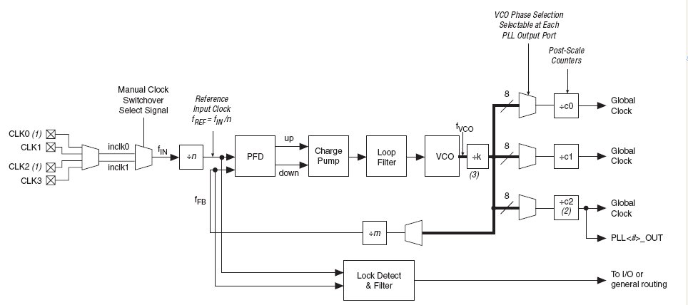 .
.
The internal distribution of the 4 PLL is 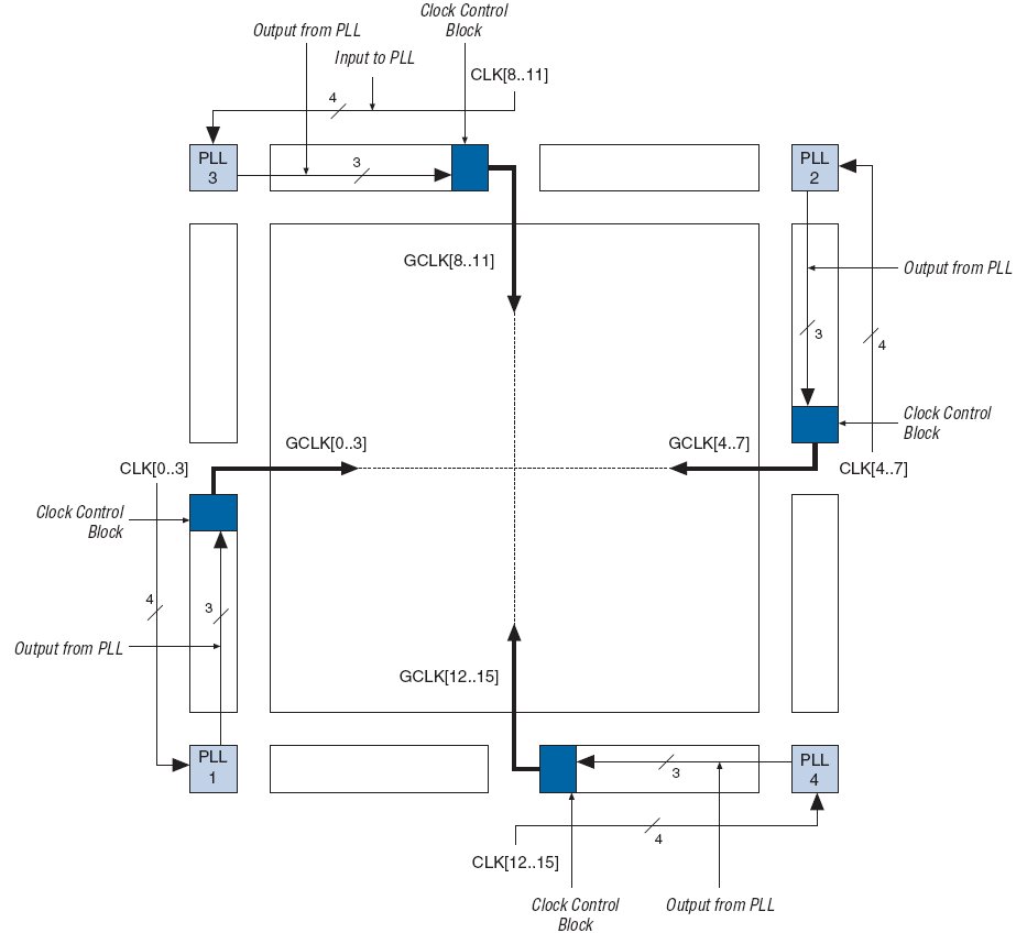
PLL component
To add a PLL component to a schematic, add it with MegaWizard Plug-In Manager and select Create a new custom megafunction variation". Select VHDL and specify a name for your PLL (ex. PLL1).
In Installed Plug-ins --> I/O --> ALTPLL
And generate the appropriate value from a 24MHz input frequency. Don't forget to select c2 output.
Exemple with 2 PLL for Clk, SDRAM and LAN:
Warning: in some cases they are some problems with the reset and Pll synchronization, especially with the LAN interface. We need to be sure that the Clk is stabilized before leaving the reset state.
Thus it could be safer to add the Pll lock output activated to leave the reset state.