Fpga4rf
From Fpga4u
Contents
About FPGA4RF
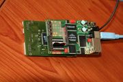
The FPGA 4 Radio Frequency is an extension board for the FPGA4U which contains a high speed DA & AD converter (Analog Devices AD9862 : two 10/12bits 64 MSPS ADCs, and two 12/14bits 128 MSPS DACs with differential analog input and output). It is connected to the FPGA4u board with the bottom 64pin connector.
The mercurial repository which contains all code is readable by everyone, and can be found at [1]. You may use
hg clone http://hg.mpb.li/fpga4rf/
to get a working copy of it. It contains the gnuradio module (gr-fpga4rf), example python scripts using it, FPGA designs (fpga4rf#firfilter firfilter is the most recent one), the pin assignments for the board, the patched fx2 firmware(usb/fx2fw-sdcc-spi), and example C programs to interact with it (usb).
A copy of the Altium design project (not always the latest version) is available here: http://mpb.li/pub/fpga4rf-altium-2008-07-25.tar.gz Keep in mind that the first revision has been incorrectly wired, and the connector is turned around by 180°. The FPGA pin assignment depends on that, and is correct for the wrong board. No corrected boards have been produced, however, there is a corrected PCB layout in the archive.
Goal
One goal is to enable the user to use the FPGA to work with radio frequency signals and to create a Software Defined Radio platform, which is usable with the GNURadio framework. GNURadio's official platform, the USRP, is rather similar to the FPGA4RF (same converter, also has Altera FPGA, FX2), and was an inspiration for this project.
The other goal is to create a basis for further developments/projects, which can extend the functionality of the existing platform. The TODO list below mentions some ideas that could be implemented.
TODO list
- Improve the GNUradio module (multiple sources : complex/floats/...)
- Create other RF frontends (design PCBs)
- Get TX to work (needs frontend, other FPGA design, and gnuradio module modifications)
- Receive or transmit (and possibly modulate/demodulate in FPGA) some real stuff :
- Reception of existing signals (AM broadcast works)
- Data transmission between two boards
- DAB/DRM/FM receiver / transmitter ( www.opendigitalradio.org )
- GPS receiver ( www.gps-sdr.com for USRP)
- Satellite pictures from weather satellites
- Other crazy idea nobody before you ever dared to think about
FPGA4RF is a project by Matthias Philippe Brändli
Conceptual description
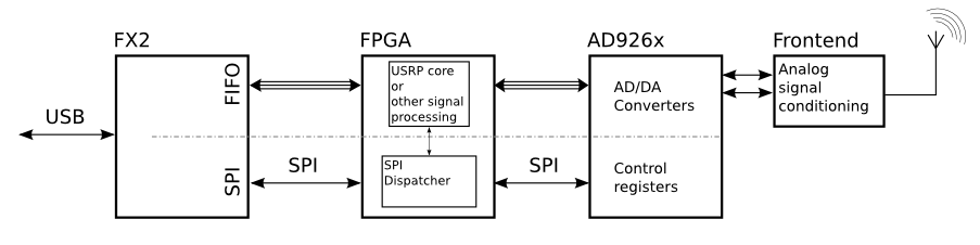
The communication path between the FX2, the fpga and the AD converter is split in two parts: a data path (upper part of block schematic), where RX and TX samples are exchanged, and a control path (SPI, lower part of block schematic), used to access to the configuration registers in the fpga and in the converter.
Data path
... described from the RF part to the USB :
The analog sides of the converters are connected to interchangeable frontends, whose purpose is to interface the FPGA4RF to the antennas or to other devices, for instance :
- signal generators, for testing of the RX path
- oscilloscopes, spectrum analysers, for testing the TX path
- down/upconverters, if the FPGA4RF is to be used at intermediate frequencies (e.g. receiving the FM broadcast band using the 10.7 MHz IF from a HiFi FM-tuner)
- whatever comes to your mind, receiving or sending signals up to 30MHz.
For now, only a simple baseband (no frequency conversion) receive frontend has been made, which has a coaxial 50Ohm input.
The FPGA must interface the AD converter and the FX2 USB controller. Depending on the clock speed given to the converter, the FPGA might need to decimate the data so that it can be transferred through USB, it's bandwidth not being large enough.
The data is being transferred using bulk data USB transfers.
On the computer, the data can be accessed using GNURadio, which allows the user to design a signal processing system using python code. A simple program which dumps all samples to a file would be like
#!/usr/bin/env python
from gnuradio import gr
import fpga4rf

class top_block(gr.top_block):
    def __init__(self):
        gr.top_block.__init__(self)
        self.build_graph()

    def build_graph (self):
        src = fpga4rf.source()
        dst = gr.file_sink(2, "fpga4rf.raw") # 2 bytes per sample
        self.connect(src, dst) # connect source to destination

try:
    print("Setting up graph")
    tb = top_block()
    tb.run()
except KeyboardInterrupt:
    print("Goodbye")
Control path
The FX2 firmware has been modified to include a SPI master, which can be controlled by vendor commands.
When the FX2 is used for bulk transfers (using the FIFOs), only four wires of the PA port are unused. PB and PD wires are used for bulk transfers, PC for JTAG and PE aren't routed to the FPGA. Thus, the only ports which can be used for the SPI master are:
- PA0, used for SCLK
- PA1, SPI MOSI
- PA3, SPI MISO
- PA7, Slave select (inverted logic)
Since there is only one slave select line, the fpga contains a SPI dispatcher, which asserts up to 256 other slave select lines selected by the first byte transferred during the read or write.
The modified firmware can be found in the repository (Or a maybe older version here: File:Fx2fw-sdcc-spi-2009-02-04.zip). Compilation and programming instructions are on the FX2 page.
To issue vendor commands, ctrl_message has been modified : File:Ctrl msg-2008-12-12.zip. Also, usr/spi_ctrl in the repository is more recent, and can read and write registers in the AD9862. (Older version : File:Spi ctrl-2009-02-04.zip)
The firmware understands the following new vendor commands: (constants are defined in spi.h)
OUT request:
- VEN_SPI_WR 0x99 - writes data to an SPI slave
IN requests:
- VEN_SPI_EN 0x96 - enables the FX2 tri-state on the four wires used for SPI
- VEN_SPI_DIS 0x97 - disables the FX2 tri-state
- VEN_SPI_RD 0x98 - reads from an SPI slave
reads and writes can be of arbitrary length. Both reads and writes first send a one-byte header (used in this project as address for the SPI dispatcher), followed by a zero to two bytes header. It then reads/writes a specified length from/to a char buffer. It can thus also be used for other applications.
SPI dispatcher
The SPI dispatcher behaves like a normal SPI slave, but does nothing else than read the first byte of a SPI bus access, and asserts another slave select pin until the access ends.
Practically, instead of asserting the slave select wire of the slave you want to transmit to, you assert the only slave select you have, send an address (the spi dispatcher asserts the correct slave select for you), send your intended data to the slave, and deassert the slave select.
The SPI_dispatcher is included in the test design File:Fx2 spi test-2009-02-04.zip. It is also used in the firfilter FPGA design.
firfilter
This is the most recent fpga design. The AD9862 is sampled at 32MSps. The samples are multiplied with an quadrature NCO (whose frequency can be controlled by SPI), and then low-pass filtered and decimated by a factor 125.
It is possible to choose between single-channel data (enabling only one side of the I/Q path) and complex I/Q samples (which are interlaced before being sent through USB2.0).