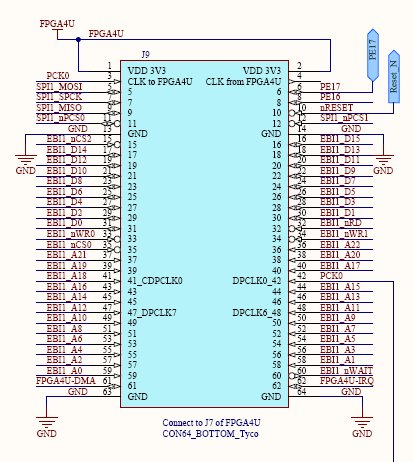
64 pins connector to FPGA4U
The FPGA4U bottom (male) connector is connected to the FPGARM4U top connector(female).

64 pins extension connector
ARM controller connections
- Extension Bus Interface 1 (EBI1) with:
- A[22..0] Byte address
- D[15..0] 16 bits data bus, tri-state bus, bidirectionnal,
- Write direction: From ARM to FPGA
- Read direction: From FPGA to ARM
- nCS0 One Mapped area of 8MBytes, start ARM adddress: 0x7000 0000
- nCS2 One Mapped area of 8MBytes, start ARM adddress: 0x9000 0000
- nRD, select read access on D[15..0]
- nWR0, select Write access on D[7..0]
- nWR1, select write access on [D15..D8]
- nRD, select read access
- nWR, select write acces
- nBS0, select access on D[7..0] (read or write)
- nBS1, select access on [D15..D8](read or write)
- A0 not available (nBS0 use the same pin)
- nWAIT, from FPGA to ARM to insert wait state cycles for the current access
- Interruptions
- FPGA4U-IRQ, to send an interrupt from FPGA to ARM
- DMA
- FPGA4U-DMA, to send a request to the RAM for DMA transfers
- Clock
- PCK0, clock from ARM4U board to FPGA
- To PLL through CLK_from_bottom (FPGA PIN_M22)
- To global input Clock pin DPCLK0 (FPGA PIN_J1)
- Reset, it's possible to Reset the ARM board from FPGA4U
- nReset connected to SWITCH1[5] !!
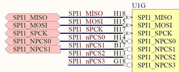
- SPI interface, master or slave from SPI1 interface with 2 Slave select
- SPI1_nPCS0
- SPI1_nPCS1
- SPI1_SPCK
- SPI1_MOSI
- SPI1_MISO
- Parallel Port PE, 2 free pins I/O
Connector assignment
Top connector on FPGARM4U, Bottom on FPGARM4U
Port 64 Pin plug Table
| Pin Num
|
FPGA Pin
|
FPGA Name
|
Alternate function
|
FPGARM4U function
|
FPGARM4U Alt/fct.
|
AT91SAM9263 Pin
|
| 2
|
|
3.3V
|
|
3.3V
|
|
|
| 4
|
PIN_E19
|
CLK_to_Conn
|
|
CLK from FPGA4U
|
|
|
| 6
|
PIN_C7
|
SWITCH1[1]
|
|
PE17
|
|
N5
|
| 8
|
PIN_E8
|
SWITCH1[3]
|
|
PE16
|
|
N6
|
| 10
|
PIN_H10
|
SWITCH1[5]
|
|
nReset
|
from STM811
|
V7
|
| 12
|
PIN_F11
|
SWITCH1[7]
|
|
SPI1 nPCS1
|
PB.16
|
B17
|
| 14
|
|
Gnd
|
|
GND
|
|
|
| 16
|
PIN_C20
|
LED[94]
|
|
EBI1_D15
|
|
R13
|
| 18
|
PIN_D20
|
LED[92]
|
|
EBI1_D13
|
|
U12
|
| 20
|
PIN_E20
|
LED[90]
|
|
EBI1_D11
|
|
V12
|
| 22
|
PIN_G22
|
LED[88]
|
|
EBI1_D9
|
|
N12
|
| 24
|
PIN_H19
|
LED[78]
|
|
EBI1_D7
|
|
T11
|
| 26
|
PIN_J22
|
LED[76]
|
|
EBI1_D5
|
|
V11
|
| 28
|
PIN_J18
|
LED[74]
|
|
EBI1_D3
|
|
U11
|
| 30
|
PIN_K21
|
LED[72]
|
|
EBI1_D1
|
|
R10
|
| 32
|
PIN_D2
|
LED[62]
|
|
EBI1_nRD
|
|
U10
|
| 34
|
PIN_E2
|
LED[60]
|
|
EBI1_nWR1
|
EBI_nBS1
|
V10
|
| 36
|
PIN_F2
|
LED[58]
|
|
EBI1_A22
|
|
N9
|
| 38
|
PIN_G5
|
LED[56]
|
|
EBI1_A20
|
|
V9
|
| 40
|
PIN_H3
|
LED[46]
|
|
EBI1_A17
|
|
R9
|
| 42
|
PIN_J1
|
LED[44]
|
DPCLK0/ DQS0L
|
PCK0
|
PWM2
|
C11
|
| 44
|
PIN_R6
|
LED[42]
|
|
EBI1_A15
|
|
V8
|
| 46
|
PIN_U3
|
LED[40]
|
|
EBI1_A13
|
|
R8
|
| 48
|
PIN_M18
|
LED[30]
|
DPCLK6/ DQS1R
|
EBI1_A11
|
|
N8
|
| 50
|
PIN_P18
|
LED[28]
|
|
EBI1_A9
|
|
V7
|
| 52
|
PIN_R21
|
LED[26]
|
|
EBI1_A7
|
|
T7
|
| 54
|
PIN_R17
|
LED[24]
|
|
EBI1_A5
|
|
U7
|
| 56
|
PIN_U21
|
LED[14]
|
|
EBI1_A3
|
|
V6
|
| 58
|
PIN_V21
|
LED[12]
|
|
EBI1_A1
|
|
V5
|
| 60
|
PIN_W21
|
LED[10]
|
|
EBI1_nWAIT (PerB)
|
PE.20
|
P6
|
| 62
|
PIN_Y19
|
LED[8]
|
|
FPGA4U-IRQ
|
|
R5
|
| 64
|
|
Gnd
|
|
GND
|
|
|
|
| Pin Num
|
FPGA Pin
|
FPGA Name
|
Alternate function
|
FPGARM4U function
|
FPGARM4U Alt/fct.
|
AT91SAM9263 Pin
|
| 1
|
|
3.3V
|
|
3.3V
|
|
|
| 3
|
PIN_M22
|
CLK_from_bottom
|
|
PCK0
|
PWM2
|
C11
|
| 5
|
PIN_H7
|
SWITCH1[0]
|
|
SPI1_MOSI
|
PB.13
|
H15
|
| 7
|
PIN_G8
|
SWITCH1[2]
|
|
SPI1_SPCK
|
PB.14
|
H17
|
| 9
|
PIN_F9
|
SWITCH1[4]
|
|
SPI1_MISO
|
PB.12
|
H18
|
| 11
|
PIN_H11
|
SWITCH1[6]
|
|
SPI1_nPCS0
|
PB.15
|
H14
|
| 13
|
|
Gnd
|
|
GND
|
|
|
| 15
|
PIN_C22
|
LED[95]
|
|
EBI1_nCS2
|
|
U13
|
| 17
|
PIN_D22
|
LED[93]
|
|
EBI1_D14
|
|
T12
|
| 19
|
PIN_E22
|
LED[91]
|
|
EBI1_D12
|
|
R12
|
| 21
|
PIN_F21
|
LED[89]
|
|
EBI1_D10
|
|
P13
|
| 23
|
PIN_G18
|
LED[79]
|
|
EBI1_D8
|
|
R11
|
| 25
|
PIN_H17
|
LED[77]
|
|
EBI1_D6
|
|
N11
|
| 27
|
PIN_J20
|
LED[75]
|
|
EBI1_D4
|
|
P12
|
| 29
|
PIN_J15
|
LED[73]
|
|
EBI1_D2
|
|
N10
|
| 31
|
PIN_C2
|
LED[63]
|
|
EBI1_D0
|
|
T10
|
| 33
|
PIN_D4
|
LED[61]
|
|
EBI1_nWR0
|
EBI_nWE
|
P11
|
| 35
|
PIN_E4
|
LED[59]
|
|
EBI1_nCS0
|
|
P10
|
| 37
|
PIN_F4
|
LED[57]
|
|
EBI1_A21
|
|
M9
|
| 39
|
PIN_H1
|
LED[47]
|
|
EBI1_A19
|
|
P9
|
| 41
|
PIN_H5
|
LED[45]
|
CDPCLK0/ DQS2L
|
EBI1_A18
|
|
T9
|
| 43
|
PIN_J4
|
LED[43]
|
|
EBI1_A16
|
|
U9
|
| 45
|
PIN_R8
|
LED[41]
|
|
EBI1_A14
|
|
R7
|
| 47
|
PIN_L18
|
LED[31]
|
DPCLK7/ DQS0R
|
EBI1_A12
|
|
T8
|
| 49
|
PIN_N21
|
LED[29]
|
|
EBI1_A10
|
|
U8
|
| 51
|
PIN_P15
|
LED[27]
|
|
EBI1_A8
|
|
P7
|
| 53
|
PIN_R19
|
LED[25]
|
|
EBI1_A6
|
|
N7
|
| 55
|
PIN_T21
|
LED[15]
|
|
EBI1_A4
|
|
P8
|
| 57
|
PIN_U19
|
LED[13]
|
|
EBI1_A2
|
|
R6
|
| 59
|
PIN_V19
|
LED[11]
|
|
EBI1_A0
|
EBI_nBS0
|
U6
|
| 61
|
PIN_Y21
|
LED[9]
|
|
FPGA4U-DMA
|
|
T6
|
| 63
|
|
Gnd
|
|
GND
|
|
|
|


